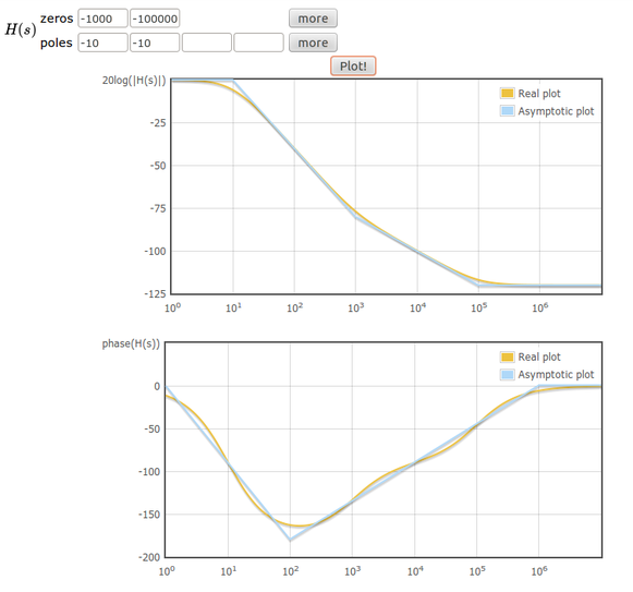
In On My Ph.D. bode plot, you can insert the zeros and poles of a transfer function and the page will draw the accurate and asymptotic bode plots of that transfer function. You can add as many zeros and poles as you like. Enjoy!
|
In On My Ph.D. bode plot, you can insert the zeros and poles of a transfer function and the page will draw the accurate and asymptotic bode plots of that transfer function. You can add as many zeros and poles as you like. Enjoy!
1 Comment
Make significant nodes easily accessible It will certainly happen that you are working to understand why something is not functioning and you want to measure a signal inside the PCB. Before developing the PCB, you might want to think which points are going to be useful to troubleshoot your circuit and, if they are not easily accessible, insert a test point somewhere connected with them. There are a number of kinds of test points, yet those that form a loop are good for test probes with hooks. Allow space between parts It is tempting to compress the components as close as they can, to just recognize that there is no space for the routing of wires. Give some distance between components to ensure that wires may spread. The more pins the part has, the more area it will be required. Spacing does not just simplify auto-routing as it will make soldering less complicated. Set parts with the same alignment Components often have a standard pin numbering, with pin #1 in the upper-left corner. In case all parts are oriented equally, you will not go wrong when soldering or when you are analyzing a component. Print the layout to see if components' dimensions match After laying out every component, print out the layout. Place each component on top of the layout sheet to check if they match. Every now and then datasheets have a typing error. Exchange wiring directions between layers Lay out vertical traces on one side and horizontal traces on the other. This helps with wiring of lines having to cross over the others. For multiple layers, interchange between directions. Select the width of lines depending on current Larger width reduces resistance, which in turn will reduce the heat caused by dissipation. The width of the lines should be sized based on the estimated current that flows through them. You can use this online calculator to determine their width. Therefore, power supply lines should be wider since all the current is supplied by these wires. Know the specifications of the board manufacturer Every supplier has its specs, such as minimum trace width, distance, quantity of layers, etc. Before starting layout, you should look at the specs you need and find a manufacturer that best matches your needs. Your requirements also include the quality of materials of the PCB. There are grades ranging from FR-1 (paper-phenolic mixture) up to FR-5 (glass cloth and epoxy). Most PCB prototyping producers employ the FR-4, but FR–2 is commonly employed in high-volume consumer applications. The type of material affects the circuit board's strength, durability, moisture absorption and Flame Resistance (FR). Do not do 90º angles with lines Sharp right angle turns are problematic to retain the trace width constant. This is a problem for thin traces, in which a tiny difference makes a meaningful fraction of the trace. A good solution is to do a pair of 45º bends. Draw on the silk layer This layer is quite standard in professional PCB providers and it is very helpful for labeling. Label the parts (the PCB layout software generally makes this) and attach a bit of information regarding what the board refers to, a revision number, and the author/owner. Employ the schematic vs. layout comparison Many PCB layout applications possess a comparison tool between schematic and layout. Make use of it to ensure that the layout is matching the schematic. Form a ground plane Specifically in analog circuits, it is important that "ground" means the exact same voltage all across the PCB. If you use traces to route the ground signal, their resistance will create voltage drops that will make distinct "grounds" in the PCB have different potentials. To avoid that, make sure you form a ground plane, i.e., a large area of copper (or even better, dedicate a layer for the plane) where the components connecting to ground can do it directly with vias. The ground plane can be totally filled with copper (better for heat dissipation) or in a square grid. One of the disadvantages of a plane is the difficulty to solder a component, considering the heat will get dissipated quickly through the ground plane. To reduce this, the contacts to planes can be achieved through thin traces. Place bypass capacitors Bypass capacitors filter AC components from your constant supply of power. They minimize noise, ripples along with other unwanted AC signals. They do so by bypassing these AC fluctuations to ground, which gives them the title. For this reason, they are often hooked between whatever voltage we want to filter (supply voltage, reference signals, etc.) and ground. A common place to put these kind of capacitors is at the power inlet to your PCB: the leads connecting the power supply to your PCB are normally long and work as antennas, collecting plenty of RF signals. One other good place is near the ICs (as near as possible to the power and ground pins), to reduce any noise injected inside your PCB. The same holds true for reference pins, or another pin where you want a very stable voltage. The value of the capacitors depend on the frequencies of the AC components. Each capacitor possesses its own frequency response defined by its resistance and Equivalent Series Inductance (ESL) that is tuned to a range of frequencies. For instance, to filter low frequencies you need a larger capacitor. Typically, a capacitor of 0.1-1µF suffices for the mid-range frequencies, if you have slow variations, you may choose around 1-10µF and for high-frequency noise you can use 0.001-0.1µF capacitors. It is possible to apply any mixture of bypass capacitors to eliminate a larger choice of frequencies. For ICs that consume more current, you may apply 10 µF - 100 µF capacitors to work as buffers. So long as the value of the capacitor allows, use monolithic ceramic capacitors since they are compact and inexpensive. Path the differential signal traces in parallel Differential signals are often used to increase immunity to noise and amplify the dynamic range. This is only effective in case that the traces of both signals follow the same paths, to make sure that the noise influences both paths identically. With that end, the two lines of a differential signal need to be parallel to the other and as near as possible. Be concerned about regions of high temperatures High temperature may degrade operation of circuits or perhaps damage them, if they are not effectively dissipated. Analyze which parts consume more power and how the heat released will be diverted by the package. The datasheet provides a parameter generally known as "Thermal Resistance" that says how much temperature raises per Watt of power considering particular conditions. The conditions may be for example with a copper area of x by y mm underneath the IC. For greater heat dissipation, you may want to put heat sinks or maybe even a fan to cool down the IC. Moreover, retain critical components of the circuit board far from these heat sources. Solder from small to large components
If you start soldering larger components, they may block access to solder the following components. You should start from the smaller components, like Surface Mount Devices (SMD) and end with the larger parts, something like through-hole capacitors or terminal blocks. |
AuthorWrite something about yourself. No need to be fancy, just an overview. ArchivesCategories |
 RSS Feed
